
The latest news
“Revolutionizing Photonic Integration & Packaging: Vanguard Automation’s SONATA 1000 is Now Available at Tyndall National Institute”
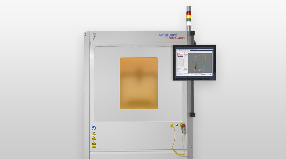
Karlsruhe, Germany, April 15, 2024 — Vanguard Automation, a Mycronic company, is delighted to announced today that its 3D lithography system, SONATA 1000, has been successfully commissioned at Tyndall National Institute. The PIXAPP pilot line, headquartered at Tyndall National Institute, consists of a highly interdisciplinary team of Europe’s leading industrial & research organizations. PIXAPP offers standardized Photonic Integrated Circuit (PIC) packaging services to customers, increasing access and reducing the cost of manufacturing photonic devices. The installation of the SONATA 1000 will advance Tyndall & PIXAPP’s mission to „break the packaging cost barrier“ by accelerating the development and commercialization of photonic integration and packaging processes.
The vanguard SONATA 1000 is a next generation technology platform, enabling automated photonic integration and packaging. The solution is scalable from low volume R&D and prototyping work, up to volume production applications. The unit is comprised of a 3D lithography-based nano fabrication system and is compatible with industry simulation software. The SONATA 1000 can print virtually any micro-optical element and can fabricate Photonic Wire Bonds™ (PWB), providing low loss interconnects between photonic components. The solution removes the need for high-precision mechanical alignment and the use of additional micro-optical elements for mode-matching.
Tyndall facility users and industry partners will benefit from using this system to both advance and accelerate their research and development activities. The vanguard SONATA 1000 will enable reliable and repeatable fabrication of multi-chip photonic subassemblies for various applications areas such as telecom / datacom, optical and quantum computing.

Tyndall’s Vanguard Automation SONATA 1000 and Personnel, left-to-right: Padraic Morrissey (Tyndall, PIXAPP Technical Manager), Sharon Butler (Tyndall, Postdoc Researcher), Matthew Hall (Tyndall, Postdoc Researcher), Kamil Gradkowski (Tyndall, Postdoc Researcher), Saif Wakeel (Tyndall, Photonics PhD Student), Laura Horan (Vanguard Automation, Staff Engineer – Product Management Lead)
Vanguard Automation signs Agreement to join the Swedish High-Tech Group Mycronic
Karlsruhe, March 22, 2024 – Vanguard Automation GmbH, a developer of technology and automated equipment for 3D nano-printing of photonic interconnects, has signed an agreement to join Mycronic, a Swedish high-tech group, listed on NASDAQ OMX Stockholm.
Mycronic is engaged in the development, manufacturing, and marketing of world-leading and innovative production solutions for the electronics industry. Mycronic is headquartered in Täby, north of Stockholm and the Group has subsidiaries in China, France, Germany, Japan, Mexico, Singapore, South Korea, the Netherlands, United Kingdom, the United States, and Vietnam.
Vanguard Automation’s area of expertise is adjacent to and complementing that of the die bonding business line in Mycronic’s Global Technologies division. With the addition of Vanguard Automation, Mycronic can offer a wider range of die bonding and photonic packaging related solutions to its customers.
“Joining the Mycronic group marks a pivotal milestone for Vanguard Automation in its mission to deploy 3D nano-printing solutions in volume production for cutting-edge photonic devices. We are looking forward to joining forces with Mycronic’s Global Technologies division, enriching the offerings to our global customer base”, says Thorsten Mayer, CEO at Vanguard Automation.
“Megatrends such as AI, cloud computing and augmented reality are boosting demand for computational power, leading to larger, more energy-intensive data centers. Vanguard Automation’s unique solutions will help speed up photonic interconnects and cut energy consumption at the same time”, says Magnus Marthinsson, Sr VP Global Technologies at Mycronic.
The transaction is expected to be finalized in April 2024, after which Vanguard Automation will form a new business line within the Global Technologies division.
Plug-and-Play Fiber-Coupled Quantum Dot Single-Photon Source via Photonic Wire Bonding
Single-photon sources are important components in the field of quantum information science. They are good candidates for the creation of critical building blocks for quantum key distribution, quantum computing, and quantum networks. During the last two decades, semiconductor quantum dots (QDs) have emerged as efficient single-photon sources with low multiphoton contribution, being able to generate on-demand single photons with near unity indistinguishability. In combination with waveguides, they offer the possibility for generating and manipulating photonic states on-chip.
Nevertheless, despite intensive research efforts aimed at achieving the collection of every single photon into a defined optical mode, coupling or interfacing on-demand single-photon sources at cryogenic temperatures with efficiencies close to unity remains an unresolved challenge. Efficient coupling to optical fibers is particularly desirable in this regard, due to their low loss, and highbandwidth transmission capabilities over long distances. Different fiber-coupling methods for single-photon sources have been extensively researched. For instance, some groups employed an epoxy method to attach a fiber, while others utilized a nanobeam attached to a tapered fiber, a graded index lens assembly in combination with a nanowire waveguide to couple light to a single-mode fiber, a bullseye design attached to the end of a single-mode fiber, evanescent coupling to a μ-fiber or a 3D printed fiber chuck and a microlens. Nevertheless, these methods are often not optimized for resonant excitation and suffer from limited scalability as well as rather high multiphoton contributions and placement accuracies in the μm range. A recently published work (ref.) gives a more detailed overview of the variety of different fiber-coupling methods described. Herein, we explore the use of photonic wire bonds (PWBs), which are flexible interconnections with low insertion loss for laser-to-chip and fiberto-chip integration. They also have been applied in hybridintegrated compact optical transceivers. Furthermore, PWBs have been employed to address the complex packaging requirements of neuromorphic photonic accelerator architectures.

a) 3D sketch of the waveguide-PWB-fiber array assembly and measurement. Laser excitation from the top through a lens (yellow) and collection via a single-mode fiber array connected via the PWB (dark yellow). Schematic view of the layer structure of the waveguide (inset).
b) Zoom to the final PWB structure from SEM imaging, connecting a waveguide to a single-mode fiber.
c) SEM image of the fiber array and a PWB connected to a ridge waveguide. An optical micrograph of the connection from the waveguide to the PWB via anchor pads is shown in the inset.
Vanguard Automation delivers Advanced Photonic Integration & Packaging Capabilities to Harvard Center for Nanoscale Systems.
Supported by the U.S. National Science Foundation (NSF)-MRI program, the Center for Nanoscale Systems (CNS) -Nanofabrication Facility at Harvard University has acquired Vanguard Automation’s SYMPHONY, a fully automated photonic integration and packaging solution enabling optical connectivity via Photonic Wire Bonding (PWB) and Facet-Attached Micro Lenses (FAML).
Karlsruhe, Germany, February 8, 2024 — Vanguard Automation (VA) announced today the commissioning of its SYMPHONY system at the Center for Nanoscale Systems (CNS) at Harvard University, a leading nanofabrication facility focused on design and fabrication of nanoscale structures, and their integration into large and complex interacting systems. This equipment installation will advance CNS’s mission of fabricating and characterizing nanoscale devices and structures. The vanguard SYMPHONY is a next generation technology platform for photonic packaging and integration, enabling automatic fabrication of low loss interconnects between photonic components, removing the need for high-precision mechanical alignment and additional micro-optical elements for mode-matching. The solution is scalable from low volume R&D and prototyping work, up to volume production applications.
VA’s SYMPHONY system facilitates its users to reliably and repeatably fabricate multi-chip photonic subassemblies in various applications areas such as telecom / datacom, optical and quantum computing. Industry partners will benefit from using this system to both advance and accelerate their research and development activities. VA’s SYMPHONY is comprised of a 3D lithography-based nano fabrication unit and automated pre- and postprocessing unit, software to enable automated and adaptive fabrication of structures and material handling as well as compatibility with industry simulation software. The equipment can print virtually any micro-optical element and can fabricate lenses and Photonic Wire Bonds™ (PWB). PWBs are freeform, low loss optical waveguide structures connecting optical devices.
“We are excited to bring 3D-nanoprinting technology to Harvard,” said Dr. Jiangdong Deng, Associate Director at Center for Nanoscale Systems (CNS), Harvard. “The Vanguard Automation system will enable engineers and researchers to rapidly evaluate and characterize advanced 3D-lithography based packaging and integration technologies in photonics research. Having access to production grade solutions will continue to drive collaboration with leading technology companies.”
“The installation of our SYMPHONY system at Harvard’s Center for Nanoscale Systems marks a significant milestone for our company,” stated Thorsten Mayer, CEO of Vanguard Automation. “The availability of this equipment at Harvard CNS will give photonics industry users, including many telecom / datacom, optical, and quantum computing organizations in the North-East corridor access to advanced photonic packaging tools.”

September 13, 2023: PIC Magazine – Issue 3, 2023
Photonic integration and packaging with Photonic Wire Bonding and facet-attached micro-optical elements
The rapid growth of photonic integrated circuits is driving the need for fast innovation, and this is made possible by the development of Photonic Wire Bonding (PWB), which creates low-loss, 3D free-form connections between optical components. Just as electrical integrated circuits have benefitted from electronic wire bonding, photonics innovations will now advance on a faster trajectory with PWB.
Built on advanced 3D nano-printing technology, PWB is inherently a fully automated process and provides a high degree of design flexibility.
.pdf - Adobe Acrobat Reader (64-bit)")
Cryogenic Optical Packaging Using Photonic Wire Bonds
In this paper, our partner at UBC, Professor Lukas Chrostowski and team use photonic wire bonding (PWB) to make reliable and efficient optical connections between single mode fiber (SMF) and silicon photonic circuits down to 970 mK.
The results presented show that PWBs can be used at such low temperatures with low loss, high bandwidth, and mechanically robust performance. This method alleviates the strict alignment challenge that occurs during assembling and cool down experienced by other packaging methods. Additional features such as UHV, vacuum bakeout compatibility and robustness to thermal cycling make PWB a promising new photonic packaging technique for a wide range of applications and operating conditions.

(a) Optical input from one fiber is guided to the surface taper through the PWB and coupled into the MRR. Light is coupled out through the other fiber port. The cool down and warm up measurement for MRR B (circled in red) is shown on the right: the calibrated transmission of two PWBs connected to a MRR (b) before cool down at 300 K vs after cool down at 5 K (c) before vs after maintaining at 5 K for 17 hours (d) before cooling down at 300 K vs after warming from 5 K at 300 K. The change in the temperature of the ring is evident from the shift in resonance wavelength. The transmission remains approximately the same through the cool down and warm up process.
Rochester Institute of Technology and Vanguard Automation Bring Advanced Photonics Packaging Capability to Rochester for High Performance Computing, Communication And Sensing
Kate Gleason College of Engineering at the Rochester Institute of Technology has acquired Vanguard Automation’s SONATA 1000, a fully automated 3D Lithography system for enabling photonic integration and packaging via Photonic Wire Bonding and Facet-Attached Micro Lenses.
Rochester, New York, March 7, 2023 — Rochester Institute of Technology (RIT) announced today the acquisition and commissioning of Vanguard Automation’s SONATA 1000, a next generation technology for photonic packaging and integration. RIT is focused on solving the challenges of photonic integration of PICs, lasers and optical fibers. Vanguard Automation’s equipment for automated fabrication of Photonic Wire Bonds™ and Facet Attached Micro Lens enables low loss interconnects between photonic devices, without requiring high-precision mechanical alignment. The equipment scales from R&D and prototyping work to volume manufacturing applications.
Vanguard’s SONATA 1000 will enable researchers to predictably fabricate multi-chip photonic subassemblies in various high performance computing uses such as classical, neuromorphic, and quantum computing. The system will also be a key tool used for training a workforce in advanced photonic packaging. RIT will be using the system in courses and workshops, as well as available for faculty-researchers involved in the development of novel photonic devices.
“We are excited to bring this technology to our labs at RIT,” said Dr. Stefan Preble, Director of the Microsystems Engineering Ph.D. Program and Professor of Electrical & Microelectronic Engineering in RIT’s Kate Gleason College of Engineering. “The Vanguard Automation system will accelerate research and development in integrated photonics by enabling researchers to rapidly and flexibly integrate a wide range of photonic chip components with a high level of predictability.”
“The installation of our SONATA 1000 system at an integrated photonics stronghold like RIT marks a significant milestone for our company,” stated Thorsten Mayer, CEO of Vanguard Automation. “Dr. Preble has been instrumental in developing Rochester as a leading photonics center in the Eastern part of North America, and we are excited to have the opportunity to contribute to his efforts.”
RIT acknowledges funding support from AIM Photonics, one of the Manufacturing Innovation Institutes managed and established by the United States Department of Defense.
About Vanguard Automation GmbH
Vanguard Automation combines a decade of research in integrated photonics with 20 years of experience in building high-precision assembly machinery to propel photonic integration and packaging. Headquartered in Karlsruhe, Germany, VA develops process technology and machines for creating low-loss photonic connections between passive and active optical components leveraging its unique IP portfolio for Photonic Wire Bonding and facet-attached micro-optics. Augmenting nano-print technology, VA’s solutions enable high packaging density, increased design flexibility and fabrication throughput.
About Rochester Institute of Technology
Rochester Institute of Technology is home to leading creators, entrepreneurs, innovators and researchers. Founded in 1829, RIT enrolls 19,700 students in more than 200 career-oriented and professional programs, making it among the largest private universities in the U.S.
The university is internationally recognized and ranked for academic leadership in business, computing, engineering, imaging science, liberal arts, sustainability, and fine and applied arts. RIT also offers unparalleled support services for deaf and hard-of-hearing students. The cooperative education program is one of the oldest and largest in the nation. Global partnerships include campuses in China, Croatia, Dubai and Kosovo.

RIT’s Vanguard Automation SONATA 1000 and Personnel, left-to-right:
Venkatesh Deenadayalan (RIT, Microsystems Engineering PhD Student), Mario Ciminelli (RIT, Packaging Engineer), Stefan Preble (RIT, Professor), Juned Kemal (Vanguard Automation, Senior Applications Engineer – Technical Support Lead)
Vanguard Automation and POET Technologies Collaborate on Solutions for Co-packaged Optics and AI-ML Applications
Karlsruhe, Germany and Toronto, Ontario, March 6, 2023 — Vanguard Automation GmbH, the developer of 3D-nanoprinted Photonic Wire Bond and Micro-Lens technology and manufacturer of software-defined equipment for photonic integration and packaging and POET Technologies Inc. (“POET” or the “Company”) (TSX Venture: PTK; NASDAQ: POET), the designer and developer of the POET Optical Interposer™ and Photonic Integrated Circuits (PICs) for the data center, telecommunication and artificial intelligence markets, today announced a collaboration to enable the integration of Micro-Lenses on the POET Optical Interposer to maximize coupling efficiency while maintaining POET’s wafer-level passive assembly process.
“The number one requirement for the POET Optical Interposer is to maintain a passive, wafer-level assembly process for POET-designed optical engines and light source products. It is the key to our ability to offer significant scale and cost benefits to our customers,” said Dr. Suresh Venkatesan, Chairman & CEO of POET. “Our optical interposer together with Vanguard Automation’s Facet-Attached-Micro-Lenses creates a powerful platform for electro-optical engines for transceivers, co-packaged optics, light engines and sensing devices. Incorporating Micro-Lenses improves the coupling efficiency of light as it passes from one photonic device to another, which in turn reduces power consumption of the combined solution. The precise alignment and printing of the Micro-Lenses at wafer-level offers significant scalability and enhances our ability to address new markets with a uniquely powerful solution.”
“We are excited to collaborate with POET Technologies to implement Vanguard Automation’s photonic integration and packaging solutions,” said Thorsten Mayer, CEO and Managing Director of Vanguard Automation GmbH. “The ability to print Facet-Attached-Micro-Lenses at wafer level with POET’s Optical Interposer technology offers a unique electro-optical platform and combines the complementary strengths of both companies.”
Vanguard Automation and POET Technologies will initially collaborate to integrate the Micro-Lenses on POET’s LightBarTM products, aimed at AI-ML accelerators and bio-sensing applications to validate power efficiency improvements and the viability of chip-scale, wafer-level manufacturing using Micro-Lenses. POET expects to start sampling LightBar products incorporating Vanguard Automation’s Micro-Lenses to customers in the second half of 2023.
About Vanguard Automation GmbH
Vanguard Automation combines a decade of research in integrated photonics with 20 years of experience in building high-precision assembly machinery to propel photonic integration and packaging. Headquartered in Karlsruhe, Germany, Vanguard Automation develops process technology and machines for creating low-loss photonic connections between passive and active optical components leveraging its unique IP portfolio for Photonic Wire Bonding and facet-attached micro-optics. Augmenting nano-print technology, Vanguard Automation’s solutions enable high packaging density, increased design flexibility and fabrication throughput.
About POET Technologies Inc.
POET Technologies is a design and development company offering integration solutions based on the POET Optical Interposer™, a novel platform that allows the seamless integration of electronic and photonic devices into a single multi-chip module using advanced wafer-level semiconductor manufacturing techniques and packaging methods. POET’s Optical Interposer eliminates costly components and labor-intensive assembly, alignment, burn-in and testing methods employed in conventional photonics. The cost-efficient integration scheme and scalability of the POET Optical Interposer brings value to any device or system that integrates electronics and photonics, including some of the highest growth areas of computing, such as Artificial Intelligence (AI), the Internet of Things (IoT), autonomous vehicles and high-speed networking for cloud service providers and data centers. POET is headquartered in Toronto, with operations in Allentown, PA, Shenzhen, China and Singapore. More information may be obtained at www.poet-technologies.com.
Light: Advanced Manufacturing accepted article preview 13 January 2023
3D-printed facet-attached microlenses for advancedphotonic system assembly
Wafer-level mass production of photonic integrated circuits (PIC) has become a technological mainstay in the field of optics and photonics, enabling many novel and disrupting a wide range of existing applications. However, scalable photonic packaging and system assembly still represents a major challenge that often hinders commercial adoption of PIC-based solutions. Specifically, chip-to-chip and fiber-to-chip connections often rely on so-called active alignment techniques, where the coupling efficiency is continuously measured and optimized during the assembly process. This unavoidably leads to technically complex assembly processes and high cost, thereby eliminating most of the inherent scalability advantages of PIC-based solutions. In this paper, we demonstrate that 3D-printed facet-attached microlenses (FaML) can overcome this problem by opening an attractive path towards highly scalable photonic system assembly, relying entirely on passive assembly techniques based on industry-standard machine vision and/or simple mechanical stops. FaML can be printed with high precision to the facets of optical components using multi-photon lithography, thereby offering the possibility to shape the emitted beams by freely designed refractive or reflective surfaces. Specifically, the emitted beams can be collimated to a comparatively large diameter that is independent of the device-specific mode fields, thereby relaxing both axial and lateral alignment tolerances. Moreover, the FaML concept allows to insert discrete optical elements such as optical isolators into the free-space beam paths between PIC facets. We show the viability and the versatility of the scheme in a series of selected experiments of high technical relevance, comprising pluggable fiber-chip interfaces, the combination of PIC with discrete micro-optical elements such as polarization beam splitters, as well as coupling with ultra-low back-reflection based on non-planar beam paths that only comprise tilted optical surfaces. Based on our results, we believe that the FaML concept opens an attractive path towards novel PIC-based system architectures that combine the distinct advantages of different photonic integration platforms.

Coupling between a single-mode fiber array (FA) and an array of edge-emitting SiP waveguides using 3D-printed facet-attached microlenses (FaML, microscope image in the center).
Photonic Wirebonds (PWB) and 3D-printed freeform-lenses allow to fabricate widely-tunable, record-low “Sub-kHz-linewidth external-cavity laser (ECL) with Si3N4 resonator used as a tunable pump for a Kerr frequency comb”
Combining optical gain in direct-bandgap III-V materials with tunable optical feedback offered by advanced photonic integrated circuits is key to chip-scale external-cavity lasers (ECL), offering wideband tunability along with low optical linewidths. External feedback circuits can be efficiently implemented using low-loss silicon nitride (Si 3 N 4 ) waveguides, which do not suffer from two-photon absorption and can thus handle much higher power levels than conventional silicon photonics. However, co-integrating III-V-based gain elements with tunable external feedback circuits in chip-scale modules still represents a challenge, requiring either technologically demanding heterogeneous integration techniques or costly high-precision multi-chip assembly, often based on active alignment. In this work, we demonstrate Si 3 N 4 -based hybrid integrated ECL that exploit 3D-printed structures such as intra-cavity photonic wire bonds and facet-attached microlenses for low-loss optical coupling with relaxed alignment tolerances, thereby overcoming the need for active alignment while maintaining the full flexibility of multi-chip integration techniques.

Microscope image of the assembled ECL module. Inset (i) shows a scanning-electron microscope (SEM) image of the false-colored PWB between the RSOA and Si3N4 (TriPleX®) chip. Inset (ii) displays a microscope image of the five 3D-printed micro lenses on the fiber array.
Vol. 30, No. 26 / 19 Dec 2022 | Optics Express 46564
3D-printed facet-attached optical elements for beam shaping in optical phased arrays
We demonstrate an optical phased-array equipped with a 3D-printed facet-attached element for shaping and deflection of the emitted beam. The beam shaper combines freeform refractive surfaces with total-internal-reflection mirrors and is in-situ printed to edge-emitting waveguide facets using high-resolution multi-photon lithography, thereby ensuring precise alignment with respect to on-chip waveguide structures.

Integrated beam scanner based on an optical phase array with a 3D-printed beam shaper.
Vol. 30, No. 26 / 19 Dec 2022 | Optics Express 46602
3D-printed facet-attached optical elements for connecting VCSEL and photodiodes to fiber arrays and multi-core fibers
Multicore optical fibers and ribbons based on fiber arrays allow for massively parallel transmission of signals via spatially separated channels, thereby offering attractive bandwidth scaling with linearly increasing technical effort. However, low-loss coupling of light between fiber arrays or multicore fibers and standard linear arrays of vertical-cavity surface-emitting lasers (VCSEL) or photodiodes (PD) still represents a challenge. In this paper, we demonstrate that 3D-printed facet-attached microlenses (FaML) offer an attractive path for connecting multimode fiber arrays as well as individual cores of multimode multicore fibers to standard arrays of VCSEL or PD. The freeform coupling elements are printed in situ with high precision on the device and fiber facets by high-resolution multi-photon lithography. We demonstrate coupling losses down to 0.35 dB along with lateral 1 dB alignment tolerances in excess of 10 μm, allowing to leverage fast passive assembly techniques that rely on industry-standard machine vision. To the best of our knowledge, our experiments represent the first demonstration of a coupling interface that connects individual cores of a multicore fiber to VCSEL or PD arranged in a standard linear array without the need for additional fiber-based or waveguide-based fan-out structures. Using this approach, we build a 3 × 25 Gbit/s transceiver assembly which fits into a small form-factor pluggable module and which fulfills many performance metrics specified in the IEEE 802.3 standard.

Concept of a multi-lane transceiver assembly using 3D-printed facet-attached microlenses (FaML) for connecting linear arrays of vertical-cavity surface-emitting lasers (VCSEL) and photodiodes (PD) to fiber arrays (FA) or multicore fibers (MCF).
November 23,2022: PIC Magazine – Issue 4, 2022
Enabling next Generation Photonic Integration and Packaging Solutions with Photonic Wire Bonding (PWB) and Facet-Attached Micro-Lenses (FAML).
With the growth of photonic integrated circuits comes the need to innovate quickly. This innovation acceleration is made possible by the creation of Photonic Wire Bonding. Much as electrical integrated circuits have benefitted from electronic wire bonding, photonics innovations will now advance on a faster trajectory. Photonic Wire Bonding creates low-loss, 3D free-form connections between optical components. Built on advanced nano-print technology, Photonic Wire Bonding is inherently automatable and provides a high degree of design flexibility. Additionally, 3D nano-printing can also be used to fabricate facet-attached micro-optical elements on optical chips and fibers, allowing for low-loss coupling with high alignment tolerances and for wafer-level probing of optical devices.
Read the complete article at PIC Magazine.

As PICs promise to erupt across multiple end markets over the coming years, solving the challenge of effectively and efficiently packaging chiplet based photonic systems becomes a priority for many fabricators. Photonic Wire Bonding is being recognized as a new technology that promises to tackle these challenges while offering additional design flexibility. Want to learn more? Take a look at the latest Issue of the Photonics Spectra Magazine of Photonics Media that made Vanguard Automation GmbH’s Photonic Wire Bond technology their “cover model”.
Read the entire article on Photonics Spectra Magazine – June Issue.

With the growth of photonic integrated circuits comes the need to innovate quickly. And this innovation acceleration is made possible by the creation of Photonic Wire Bonding. Much as electrical integrated circuits have benefitted from electrical wire bonding, photonics innovations will now advance on a faster trajectory. Today, Vanguard Automation, C2MI, and AEPONYX announce plans to further this optical innovation.
Photonic Wire Bonding creates low-loss, 3D free-form connections between optical components. Built on advanced nano-print technology, Photonic Wire Bonding is inherently automatable and provides a high degree of design flexibility. Vanguard Automation, headquartered in Karlsruhe, Germany, has created this technology and offers industry-grade machinery, software, and fabrication process solutions. “We are delighted to not only see our machines used as innovation drivers,” says Thorsten Mayer, CEO of Vanguard Automation, “we are also excited to see them going into photonic production lines.”
The C2MI (MiQro Innovation Collaborative Center) in Quebec is a leading innovation center for microelectronics in Canada with a customer base extending beyond its national borders. Recognizing the potential of Photonic Wire Bonding, C2MI has Photonic Wire Bonding technology on their roadmap for inclusion into their photonics fab/assembly/test production flow. “This would be a significant expansion of our capabilities, offering interesting technological avenues. We are already working in collaboration with customers and partners on Photonic Wire Bonding concepts with great commercialization potential.” says Marie-Josée Turgeon, General Manager of C2MI.
AEPONYX, producer of photonic integrated circuit products, has worked with Vanguard Automation and C2MI to create product development accelerations. AEPONYX has created a Photonic Wire Bonding innovation process – working on their base of Silicon Nitride photonics, they have perfected the concept of hybrid integration. As Philippe Babin, CEO of AEPONYX, stated, “Hybrid integration enables us to test concepts with best of breed optical components, with speed not possible before.” “It has been a thrill working with Vanguard and C2MI on this development,” Philippe said.
There are two upcoming opportunities to learn even more about Photonic Wire Bonding and the three companies‘ innovations. First, Vanguard, C2MI, and AEPONYX will present the concepts in a Lightwave webinar with Steven Hardy on March 1st, 11am ET. You can visit the Lightwave or AEPONYX websites for registration information. Then, you can visit with Vanguard Automation, C2MI and AEPONYX at the OFC optical conference in San Diego this March.
Contacts @ business partners:
C2MI – www.C2MI.ca, Contact – marie-josee.turgeon@c2mi.ca
AEPONYX, Inc – www.AEPONYX.com, Contact – pbabin@AEPONYX.com


February 14, 2022: Vanguard Automation is packaging partner in the EU Project ELENA and expands its technology portfolio to Lithium Niobate on Insulator (LNOI). These new capabilities will benefit a broad range of applications including quantum technologies, telecom, LiDAR, and sensing.
ELENA is an acronym for the project title “European electro-optic and nonlinear PIC platform based on lithium niobate.” The project consortium aims to reinvent one of the oldest and best-known photonics materials – lithium niobate – in the form of a thin film on silicon substrates to be used as a standard PIC platform and benefit from miniaturization, cost reduction, and scalable manufacturing of PICs.
The ELENA project promises to benefit the entire photonics sector by developing the first European lithium niobate on insulator (LNOI)-based platform for photonic integrated circuits (PICs) and establishing the first open-access foundry service for LNOI technology. LNOI is a novel electro-optic and nonlinear PIC platform. It offers enhanced performance and new functionalities for ultra-high-speed telecom networks, optical signal processing, programmable PICs, sensing and spectroscopy, LIDAR applications, quantum information processing and quantum computing. ELENA is a collaborative Research and Innovation Action funded by the European Commission under the Horizon 2020 programme.


November 1, 2021: The Board of Vanguard Automation (VA) announces Thorsten Mayer as new Chief Executive Officer, effective November 1, 2021.
Thorsten Mayer will succeed Alois Hauk, co-founder and Chief Executive Officer since the company’s incorporation in September 2017. “Alois has been instrumental in helping us move our ideas and initial prototypes from the laboratory to the marketplace, establishing a joint-venture with ELAS Technologies Investment*, and leading the company from infancy to delivering the first products to an international customer base,” said Prof. Dr. Christian Koos, Co-Founder and Strategic Technology Advisor of Vanguard Automation.
Thorsten Mayer had joined Vanguard Automation in November 2020 as a Chief Operating Officer, with more than two decades of leadership experience in international high-tech industries. “We are very pleased that we won Thorsten Mayer to lead the next growth phase of Vanguard Automation.” said Alois Hauk, “He brings a wealth of international experience in high-tech sales, strategic marketing and operational management to the table. We have spent the past year working closely together to prepare a smooth transition of the Chief Executive position”. Alois Hauk will end his involvement in the operational management of the company by the end of the year and will continue to serve as an advisor on the Board.
“I am enthusiastic about the technology and its potential to revolutionize photonic packaging and assembly. Equally, I am humbled by the task ahead and the opportunity to lead and serve a group of extremely talented people. Together we have already begun laying the foundation for the next stage in our journey,” said Thorsten Mayer.
*ELAS Technologies Investment is a German-based, globally oriented financial investor, headquartered in Achim, Germany. ELAS provides financial agility and infrastructure support for promising organizations in high-tech industries such as photonics, electronics and clean-tech, to name a few.

October 21, 2021: Lukas Chrostowski, Professor at the University of British Columbia, talks about „Photonic Wire Bonding for Integrated Photonics“ at IEEE Photonics Society 2021. His talk can be watched on Youtube https://youtu.be/hEwyInEfwUw.
Lukas Chrostowski, PEng., Professor at Electrical and Computer Engineering, University of British Columbia (UBC), commissioned the Photonic Wirebonding Tool from Vanguard Automation in August 2020. Since then, Lukas‘ institute acts as a research partner for Vanguard Automation and offers process development and new applications for their customers.
 for Integrated Photonics")
August 18, 2021: Vanguard Automation will be presenting its revolutionary technology between 16. and 18. of September at the 2021 China International Optoelectronic Exposition (CIOE). The show will take place at the Shenzhen World Exhibition & Convention Center and will host leading technology companies from around the world.
“The 23. China International Optoelectronic Exposition offers us an excellent platform to reach new costumers and extend existing partnerships in the Greater China market,” says Thorsten Mayer, COO of Vanguard Automation.

Vol. 29, No. 17 / 16 Aug 2021 | Optics Express 27710
Superconducting nanowire single-photon detector with 3D-printed free-form microlenses
We present an approach to increase the effective light-receiving area of superconducting nanowire single-photon detectors (SNSPD) by free-form microlenses. These lenses are printed in situ on top of the sensitive detector areas using high-resolution multi-photon lithography. We demonstrate a detector based on niobium-nitride (NbN) nanowires with a 4.5 µm × 4.5 µm sensitive area, supplemented with a lens of 60-µm-diameter. For a plane-wave-like free-space illumination at a wavelength of 1550 nm, the lensed sensor has a 100-fold increased effective collection area, which leads to a strongly enhanced system detection efficiency without the need for long nanowires. Our approach can be readily applied to a wide range of sensor types. It effectively overcomes the inherent design conflict between high count rate, high timing accuracy, and high fabrication yield on the one hand and high collection efficiency through a large effective detection area on the other hand.

Experimental demonstration using a pair of SNSPD on the same chip. One detector is equipped with a 3D-printed lens (“lensed detector”) while the other is left blank (“reference detector”).
Scientific Reports, 12 August 2021
Hybrid external-cavity lasers (ECL) using photonic wire bonds as coupling elements
Combining semiconductor optical amplifiers (SOA) on direct-bandgap III–V substrates with low-loss silicon or silicon-nitride photonic integrated circuits (PIC) has been key to chip-scale external-cavity lasers (ECL) that offer wideband tunability along with small optical linewidths. However, fabrication of such devices still relies on technologically demanding monolithic integration of heterogeneous material systems or requires costly high-precision package-level assembly, often based on active alignment, to achieve low-loss coupling between the SOA and the external feedback circuits. In this paper, we demonstrate a novel class of hybrid ECL that overcome these limitations by exploiting 3D-printed photonic wire bonds as intra-cavity coupling elements. Photonic wire bonds can be written in-situ in a fully automated process with shapes adapted to the mode-field sizes and the positions of the chips at both ends, thereby providing low-loss coupling even in presence of limited placement accuracy. In a proof-of-concept experiment, we use an InP-based reflective SOA (RSOA) along with a silicon photonic external feedback circuit and demonstrate a single-mode tuning range from 1515 to 1565 nm along with side mode suppression ratios above 40 dB and intrinsic linewidths down to 105 kHz. Our approach combines the scalability advantages of monolithic integration with the performance and flexibility of hybrid multi-chip assemblies and may thus open a path towards integrated ECL on a wide variety of integration platforms.

Concept and realization of a hybrid external cavity laser (ECL) with a photonic wirebond (PWB) as intra-cavity coupling element.
Juli 12, 2021: Vanguard Automation has just completed the expansion of its clean room and more than doubled the space for final testing of customer systems and process development.
“In order to cope with the rapid growth of our company and serve our growing customer base with packaging processes tailored to their devices, we decided to rebuild our clean room just two years after the original installation,” says Alois Hauk, CEO of Vanguard Automation.

Light: Science & Applications (2020) 9:71
Hybrid multi-chip assembly of optical
communication engines by in situ 3D nanolithography
Three-dimensional (3D) nano-printing of freeform optical waveguides, also referred to as photonic wire bonding, allows for efficient coupling between photonic chips and can greatly simplify optical system assembly. As a key advantage, the shape and the trajectory of photonic wire bonds can be adapted to the mode-field profiles and the positions of the chips, thereby offering an attractive alternative to conventional optical assembly techniques that rely on technically complex and costly high-precision alignment. However, while the fundamental advantages of the photonic wire bonding concept have been shown in proof-of-concept experiments, it has so far been unclear whether the technique can also be leveraged for practically relevant use cases with stringent reproducibility and reliability requirements. In this paper, we demonstrate optical communication engines that rely on photonic wire bonding for connecting arrays of silicon photonic modulators to InP lasers and single-mode fibres. In a first experiment, we show an eight-channel transmitter offering an aggregate line rate of 448 Gbit/s by low-complexity intensity modulation. A second experiment is dedicated to a four-channel coherent transmitter, operating at a net data rate of 732.7 Gbit/s – a record for coherent silicon photonic transmitters with co-packaged lasers. Using dedicated test chips, we further demonstrate automated mass production of photonic wire bonds with insertion losses of (0.7 ± 0.15) dB, and we show their resilience in environmental-stability tests and at high optical power. These results might form the basis for simplified assembly of advanced photonic multi-chip systems that combine the distinct advantages of different integration platforms.

Concept and implementation of hybrid multi-chip modules (MCMs) by 3D nano-printing of photonic wire bonds (PWBs).
Vol. 27, No. 12 / 10 Jun 2019 | OPTICS EXPRESS 17402
Photonic-integrated circuits with non-planar topologies realized by 3D-printed waveguide overpasses
Complex photonic-integrated circuits (PIC) may have strongly non-planar topologies that require waveguide crossings (WGX) when realized in single-layer integration platforms. The number of WGX increases rapidly with the complexity of the circuit, in particular when it comes to highly interconnected optical switch topologies. Here, we present a concept for WGX-free PIC that relies on 3D-printed freeform waveguide overpasses (WOP). We experimentally demonstrate the viability of our approach using the example of a 4 × 4 switch-and-select (SAS) circuit realized on the silicon photonic platform. We further present a comprehensive graph-theoretical analysis of different n × n SAS circuit topologies. We find that for increasing port counts n of the SAS circuit, the number of WGX increases with n4, whereas the number of WOP increases only in proportion to n2.

Waveguide overpasses (WOP) on the silicon photonic (SiP) platform. The WOP is written into a liquid negative-tone photoresist that is deposited onto the PIC.
February 5, 2019: Vanguard Automation has introduced its SONATA1000 Series at SPIE Photonics West Exhibition in San Francisco. It’s the first industrial solution for in-situ printing of Photonic Wire Bonds (PWB) and facet-attached micro-optical elements. With Vanguard Automation, 3D printing of freeform waveguides and micro-optical elements is about to revolutionize photonic packaging and system assembly.
September 21, 2018: Various employees of Vanguard Automation and the Karlsruhe Institute of Technology (KIT) received the Second Prize of the prestigious Berthold Leibinger Innovationspreis 2018. The 10th Award Ceremony took place on September 21, 2018, in Ditzingen, Germany. More than 500 guests from all over the world participated at the event.
The encomium was held by Prof. Dr.-Ing. Wolfgang Marquardt, Chairman of the Board, Forschungszentrum Jülich.
Vol. 5, No. 7 / July 2018 | Optica 876
Hybrid integration of silicon photonics circuits and InP lasers by photonic wire bonding
Efficient coupling of III–V light sources to silicon photonic circuits is one of the key challenges of integrated optics. Important requirements are low coupling losses, as well as a small footprint and a high yield of the overall assembly, along with the ability to use automated processes for large-scale production. In this paper, we demonstrate that photonic wire bonding addresses these challenges by exploiting direct-write two-photon lithography for in situ fabrication of three-dimensional freeform waveguides between optical chips. In a series of proof-of-concept experiments, we connect indium phosphide (InP)-based horizontal-cavity surface-emitting lasers to passive silicon photonic circuits with insertion losses down to 0.4 dB. To the best of our knowledge, this is the most efficient interface between an InP light source and a silicon photonic chip that has so far been demonstrated. Our experiments represent a key step in advancing photonic wire bonding to a universal integration platform for hybrid photonic multi-chip assemblies that combine known-good dies of different materials to high-performance hybrid multi-chip modules.

Photonic multi-chip transmitter for WDM communications. The system exploits PWBs to combine the distinct advantages of different photonic integration platforms: DFB lasers are realized based on direct-bandgap InP substrates, whereas SiP chips lend themselves to implement electro-optic modulators. For dense packing of optical channels, high-quality AWGs are needed, which are best realized on medium-index-contrast material systems such as TriPleX.
Nature Photonics volume 12, pages241–247 (2018)
In situ 3D nanoprinting of free-form coupling elements for hybrid photonic integration
Dietrich et al., “In situ 3D nanoprinting of free-form coupling elements for hybrid photonic integration,” Nature Photon 12, 241–247 (2018). Read more.
Artist’s view (A to F) and experimental realizations (subfigures a to f) of various beam-shaping elements that can be used as universal building blocks for hybrid photonic multi-chip systems.
Hybrid photonic integration exploits complementary strengths of different material platforms, thereby offering superior performance and design flexibility in comparison to monolithic approaches. This applies in particular to multi-chip concepts, where components can be individually optimized and tested on separate dies before integration into more complex systems. The assembly of such systems, however, still represents a major challenge, requiring complex and expensive processes for high-precision alignment as well as careful adaptation of optical mode profiles. Here we show that these challenges can be overcome by in-situ nano-printing of freeform beam-shaping elements to facets of optical components. The approach is applicable to a wide variety of devices and assembly concepts and allows adaptation of vastly dissimilar mode profiles while considerably relaxing alignment tolerances to the extent that scalable, cost-effective passive assembly techniques can be used. We experimentally prove the viability of the concept by fabricating and testing a selection of beam-shaping elements at chip and fiber facets, achieving coupling efficiencies of up to 88 % between an InP laser and an optical fiber. We also demonstrate printed freeform mirrors for simultaneously adapting beam shape and propagation direction, and we explore multi-lens systems for beam expansion. The concept paves the way to automated fabrication of photonic multi-chip assemblies with unprecedented performance and versatility.

